Computer System Architecture - Pipeline and Vector Processing

Avatto > > UGC NET COMPUTER SCIENCE > > PRACTICE QUESTIONS > > Computer System Architecture > > Pipeline and Vector Processing

21. The stage delays in a 4-stage pipeline are 800, 500, 400 and 300 picoseconds. The first stage (with delay 800 picoseconds) is replaced with a functionally equivalent design involving two stages with respective delays 600 and 350 picoseconds. The throughout increase of the pipeline is ........ percent.

Cancel reply

Your email address will not be published. Required fields are marked *


Cancel reply

Your email address will not be published. Required fields are marked *


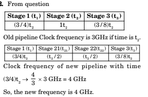
22. Consider a 3 GHz (gigahertz) processor with a three- stage pipeline and stage latencies π1, π2 and π3 such that π1 = 3π2/4 = 2π3. If the longest pipeline stage is split into two pipeline stages of equal latency, the new frequency is ......... GHz, ignoring delays in the pipeline registers.

Cancel reply

Your email address will not be published. Required fields are marked *


Cancel reply

Your email address will not be published. Required fields are marked *


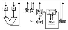
23. Consider the following data path of a simple non- pipelined CPU. The registers A, B, A1 , A2, MDR, the bus and the ALU are 8-bit wide. SP and MAR are 16-bit registers. The MUX is of size 8 × (2 : 1) and the DEMUX is of size 8 × (1 : 2). Each memory operation takes 2 CPU clock cycles and uses MAR (Memory Address Register) and MDR (Memory Data Register). SP can be decremented locally.

pipelining

The CPU instruction “push r”, where r = A or B, has the specification
M[SP] ⇽ r
SP ⇽ SP – 1
How many CPU clock cycles are needed to execute the ‘push r” instruction?

  • Option : A
  • Explanation : Push ‘r’ consist of following operations :
    M[SP ]!R
    SP!SP-1
    ‘r’ is stored at memory at address stack pointer currently is, this take 2 clock cycles
    SP is then decremented to point to next top of stack
Cancel reply

Your email address will not be published. Required fields are marked *


Cancel reply

Your email address will not be published. Required fields are marked *


24. A line L in a circuit is said to have a stuck-at-0 fault if the line permanently has a logic value 0. Similarly a line L in a circuit is said to have a stuck-at-1 fault if the line permanently has a logic value 1. A circuit is said to have a multiple stuck- at fault if one or more lines have stuck at faults. The total number of distinct multiple stuck-at faults possible in a circuit with N lines is

  • Option : B
  • Explanation : In a line, there can be three possibilities :
    1. Stuck-at 0 fault
    2. Stuck-at 1 fault
    3. No fault
    Thus, total combinations = 3N
    It is mentioned that one or more lines have stuck at faults.
    So, a case in which there is no fault in any line i.e. all lines are correct can not occur.
    Total combinations = 3N – 1
Cancel reply

Your email address will not be published. Required fields are marked *


Cancel reply

Your email address will not be published. Required fields are marked *


25. The floating point unit of a processor using a design D takes 2t cycles compared to t cycles taken by the fixed point unit. There are two more design suggestions D1 and D2. D1 uses 30% more cycles for fixed point but 30% less cycles for floating point unit as compared to design D. D2 uses 40% less cycles for fixed point unit but 10% more cycles for floating point unit as compared to design D. For a given program which has 80% fixed point operations and 20% floating point operations, which of the following ordering reflects the relative performances of three designs? (Di > Dj denotes that Di is faster than Dj)

  • Option : A
  • Explanation : 0.8 * (time taken in fixed point) + 0.2 (time taken in floating point) Say, t = 1
    D = 0.8(1) + 0.2(2)
    = 1.2
    D1 = 0.8(1.3) + 0.2(1.4)
    = 1.04 +.28 = 1.32
    D2 = 0.8(1 – 0.04) + 0.2(2 – 2*0.1)
    = 0.8 * 0.96 + 0.2 * 1.8
    = 0.768 + 0.36 = 1.128
    D1 > D > D2
Cancel reply

Your email address will not be published. Required fields are marked *


Cancel reply

Your email address will not be published. Required fields are marked *