info@avatto.com
+91-9920808017
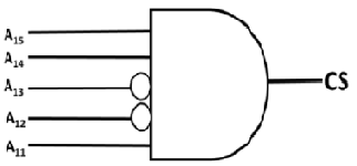
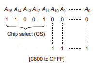
0. The chip select logic for a certain DRAM chip in a memory system design is shown below. Assume that the memory system has 16 address lines denoted by A15 to A0. What is the range of addresses (in hexadecimal) of the memory system that can get enabled by the chip select (CS) signal?
C800 to CFFF
CA00 to CAFF
C800 to C8FF
DA00 to DFFF
Your email address will not be published. Required fields are marked *
Report
Name
Email
Website
Save my name, email, and website in this browser for the next time I comment.
Comment
Login with Facebook
Login with Google
Forgot your password?
Lost your password? Please enter your email address. You will receive mail with link to set new password.
Back to login